
In
the early years of the GPU acceleration of application performance – really
from “Kepler” datacenter GPUs in May 2012 to “Volta” in May 2017 – Nvidia, the
world’s most important technology company and still the overwhelmingly dominant
supplier of hardware and systems software for the GenAI revolution, was very
good about putting out roadmaps.
But
for a few years until 2021, the company kept its roadmaps folded up in the
front left inside pocket of co-founder and chief executive officer Jensen Huang’s
leather jacket, but as the GenAI boom went from chemical to nuclear, the
company correctly surmised that with everybody trying to synchronize money, land,
power, cooling, and systems to all come together in the largest infrastructure
buildout the IT market has ever seen, everybody needed a real roadmap, extending
out a few years, so they could plan.The
first such new era roadmap came
out at the end of 2023 in a financial presentation, not in a GTC conference
slide from Huang, and we edited the heck out of it to add missing components
like the some of the GPUs and DPUs and putting the correct calendar years on the
columns, but all along being grateful Nvidia was outlining where it was at and
where it was going. We gathered up all of the roadmaps we could find between
2021 and 2023 and put
them in this story so you would have them for reference.
That
October 2023 roadmap reveal was also when we got the first wind of the annual
cadence of updates that Nvidia was scheduling for its AI system components. On this
late 2023 roadmap, the 2025 products were called the GX200, the GX200NVL, the
X100, and the X40, which had me thinking they were going to recycle the “Xavier”
codename from the gaming side of the house, but we conceded that X could also
be a variable. The 2025 products turned out to be the “Blackwell” GPUs that
were detailed by Huang at the Computex conference in June 2024 in the new-style
roadmap we by now have seen a bunch of times with additions. (The font is
pretty small for those of us of a certain age, so you might have to squint a
little.)
Nvidia
unfolded its datacenter roadmap out to 2027 in June 2024, when we learned
about the “Vera” CV100 Arm server CPUs and the “Rubin” R200 GPU accelerators
for the first time. And then Huang folded out another year and showed
us the datacenter roadmap out to 2028 at the GTC conference last year.
At
the GTC 2026 conference, Huang added some more details on the machinery between
2026 and 2028, but he did not talk about a future and likely “Feynman Ultra”
GPU expected along with updated ConnectX-10 SmartNICs and maybe even an updated
Groq LPU that could came that year, too.
Nvidia
Mostly Owns Training, And Can Compete On Inference
These
roadmaps are important to the OEMs and ODMs that convert Nvidia’s technology into
the systems that run AI training and inference for the vast majority of the
world. And also for customers, who as we all know invest in roadmaps but do not
simply acquire point products. Despite all of the glorious competition from the
Cambrian explosion in AI compute engines and networking, Nvidia by far still
has dominant market share and will for many years to come. How much remains to
be seen.
If
you do some rough math, which as you know I love to do, the total server market
in 2025 generated somewhere between $420 billion and $450 billion based on the
limited data we see out of IDC and Gartner, and about $190 billion of the bill
of materials for those systems passed through to Nvidia as revenue. Moreover, the
machines sold by the OEMs and ODMs that had at least Nvidia GPUs (and very
likely more components) installed in them probably represented somewhere
between $275 billion and $325 billion in revenues in 2025. That gives machines
based on Nvidia technologies somewhere around a low of 61 percent share to a
high of 77 percent share of the overall systems market. We have to use a
quantum probabilistic distribution to get any more accurate than that (you
were supposed to laugh there), or see all of the financials of all the
public and private server makers and add everything up.
I
guess the point is that damned near all of the profits for AI systems are going
to Nvidia, as its gross, operating, and net income clearly show.
Truly
amazing.
Which
brings us to the 2026 roadmap as presented at Huang’s GTC keynote address:

This
time around, the evolution of the “Oberon” and “Kyber” racks is being explicitly
called out alongside the evolution of the compute and networking engines.
You
will also note that Quantum InfiniBand is not mentioned, and that is not
because Nvidia is stopping development on InfiniBand but more that Nvidia does
not expect for AI factories to deploy InfiniBand even if there are cases where
HPC centers running smaller clusters or even some AI centers might opt for that.
Furthermore,
as we
pointed out in our prior coverage of Huang’s keynote, the “Rubin” CPX long
context and attenuation processing engine, which
was unveiled last September, is not on the roadmap. The Rubin CPX was
expected to be delivered at the end of this year for AI context windows of 1
million tokens or more as well as helping with video generation for models that
do pictures instead of words. It may be premature to count CPX out of the
picture for such workloads. In fact, you might see a combination of Nvidia CPX
and Groq LPU compute engines handling both kinds of inference – and Vera-Rubin
compute complexes not involved. (Nvidia did not say this, but I am.)
The
Vera-Rubin systems are locked and loaded for volume shipments in the second
half of 2026, as planned. The Vera Arm server CPU has 88 custom Nvidia “Olympus”
cores with two threads per core and a 1.8 TB/sec NVLink chip-to-chip interconnect
that can be used as a high speed connection between one or more “Rubin” R200
GPU accelerators. Rubin is, as
we know from this time last year, a pair of reticle-sized GPU chips linked
by NVLink C2C ports inside a single socket that has 288 GB of HBM4 memory and
delivers 50 petaflops of FP4 performance on its tensor cores compared to 10
petaflops for the “Blackwell” B200 and 15 petaflops for the B300. These B200
and B300 GPUs have 288 GB of HBM3E stacked memory. Rubin is expected to be etched
using the 3 nanometer N3E or N3P process from Taiwan Semiconductor
Manufacturing Co. As far as we know, the Oberon racks will have the same 72 GPU
sockets and the same 36 CPU sockets in NVL72 rackscale systems as were done in
the Blackwell generation with the B200 and B300. (Nvidia was calling these
NVL144 by counting GPU chips, not sockets for a while, confusing itself and
more than a few customers.)
Alongside
Vera and Rubin, the Groq LP30 will ship inside of dedicated racks with a regular
Spectrum Ethernet spine (sometimes called a backplane). As far as we know, this
Ethernet spine not use the Spectrum-6 ASICs with co-packaged optics, but it
could us optics in the spine and copper in the chip-to-chip spine connectors
coming off the Groq chips.
Nvidia
calls this an Oberon ETL256 configuration, which means that either 256 Vera
CPUs or 256 Groq LPUs can be linked to this backplane.
The
Groq sleds coming this year have eight LP30s in four sockets per sled, and they
look like this:
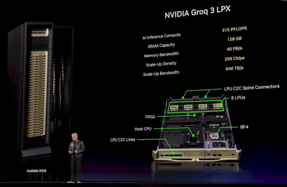
A
rack of the LP30s is called the Groq 3 LPX system, and it has 32 sleds with a
total of 315 petaflops of FP8 inference computing, 128 GB of SRAM on the 256
chips, 40 PB/sec of aggregate SRAM bandwidth, and 640 TB/sec of aggregate scale
up bandwidth across the Spectrum ETL backplane. (Again, it is not clear if this
is Spectrum-5 or Spectrum-6 with the CPO removed. We suspect it is Spectrum-5,
which is simpler.)
Later
this year, it will also be possible to get whole racks of Vera server CPUs in
the Oberon racks with the ETL spine. (Meta
Platforms is going to be an early customer for this.) If you do the math,
that is eight Vera CPUs (possibly four two-way Vera-Vera nodes) in each sled,
with 32 sleds in a Vera ETL racks. That is 256 CPUs with a total of 22,528
cores and 512 TB of main memory and 300 TB/sec of bandwidth across that memory.
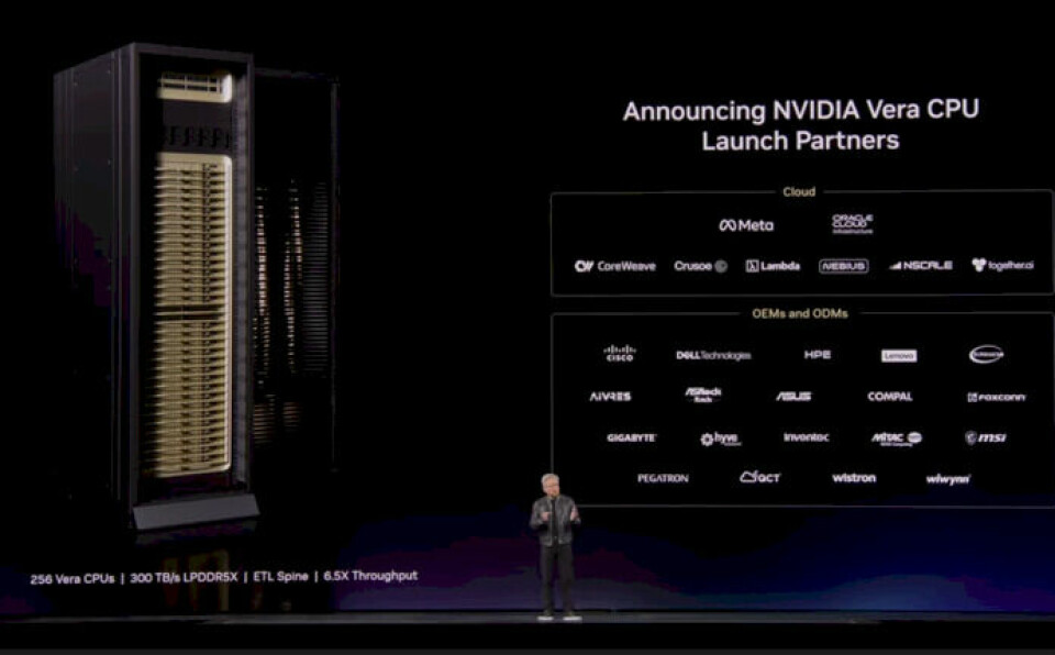
Presumably
this will be called a Vera CPX rack, with CPX being short for Compute
Processing Rack (not to be confused with the Rubin CPX processor). The storage
racks based on the BlueField-4 DPUs running various distributed storage software
stacks from a dozen or so partners is called a BlueField STX rack, and similarly
a rack of Spectrum-6 switchery is called the Spectrum-5 SPX rack.
Perhaps
the X was not a good idea in the naming. Perhaps, just perhaps, these should have
been called CPR, STX, and SPR? Naming matters. The are all based on the MGX
modular server architecture, and MGX is not to be confused with the private
equity firm in the Middle East that is underwriting a lot of AI facilities
around the globe these days.
As
we roll forward into 2027, the “Rubin Ultra” GPU, presumably called the R300, is
just a doubling up of GPU chips inside of the Rubin socket, from two to four
chips and supplying 100 petaflops of FP4 performance. Nvidia is going to double
up the number of sockets to 144 inside the new “Kyber” rack, which will have a
copper midplane instead of huge spaghettis of thousands of copper cables
cross-coupling the GPU sockets in the rack. Nvidia will have sixteen banks of
HBM4E memory against those four Rubin GPU chips, for 1 TB of capacity and 32
TB/sec. (In theory, that HBM4E memory could run at 64 TB/sec, and we are wondering
why Nvidia is gearing it down – perhaps for power consumption and heat
dissipation reasons.)
Let’s
talk about NVLink ports and NVSwitch memory fabric interconnects for a second.
The names were out of phase a bit because the initial NVLink 1.0 that debuted
with the “Pascal” P100 GPUs back in 2016 did not have a switch but rather used
a mesh interconnect to share memory across the Pascal GPUs. The names were of
the ports and switches were lockstepped with the Blackwell B300 GPUs (I think)
and going forward the chip and port generations are names in synch. Like this:
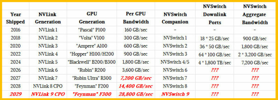
There
are many ways the NVSwitch memory fabric ASICs can be enhanced, but I think it
is safe to say that the radix – the number of ports per ASIC – is getting to be
too low and I think there is a more than even chance that Nvidia will start
thinking about not chiplets but waferscale designs for ASICs. (And might even
do that for future Groq LPUs, now that I think on it.) These would not have to
be full wafer scale, but it would mean doing away with the C2C interconnects
everywhere as well as all of the buffering that needs to be done as data moves
from one chip through the C2C interconnects and to the adjacent chips. (This
what we think secretive
networking chip startup Eridu is already working on, and Cerebras has shown
how it works well for parallel compute.)
Suffice
it to say, NVLink 6 ports on the Rubin GPUs will double to their bandwidth over
NVLink 5 ports, to 3,600 GB/sec, and they will double yet again with the Rubin
Ultra GPUs, which stands to reason given the performance doubling and the HBM4
memory bandwidth almost tripling between Rubin and Rubin Ultra.
In
the Rubin generation, the Spectrum-6 Ethernet ASICs will have co-packaged
optics, and that generation of 102.4 Tb/sec switches will also support the
scale out network needs of the Rubin Ultra systems. The 2027 Rubin Ultra product
line will see the Groq LP35 chip get FP4 floating point processing in the NVFP4
format so it matches the precision of the Blackwell and Rubin GPUs. And with
the Groq LP40 compute engine coming in the Rosa-Feynman systems in 2028, NVLink
ports will be added so the Groq engines so they can have memory coherency with
the Rosa Arm server CPUs (named after Rosalyn Sussman Yalow, a Nobel Prize
winning medical physicist who developed the radioimmunoassay method of
detecting tiny amounts of chemicals in blood or tissue) and with the Feynman
GPUs (named after famous physicist and bongo player Richard Feynman).
You
will see in the roadmap that in 2028 Nvidia will add CPO to NVLink 8 ports and
presumably for the other end at the NVSwitch ASIC. While we are always pushing
for compute engine makers to do CPO on their devices, they can be copper on
that end with a multitier network of switch ASICs using CPO on the other side.
You do not have to have CPO on both sides. (Nvidia seems to be using NVSwitch
and NVLink loosely in this chart, so be careful.) We think that CPO for
NVSwitch is interesting because it will allow for fast, high-bandwidth, two-tier
NVSwitch networks to create larger GPU compute memory domains for models to
play in.
With
Hopper GPUs, the official scalability was eight GPUs with linked memory, but
the unofficial scalability was 256 GPUs using a two tier network. With
Blackwell, the official GPU memory domain size is 72 GPUs, but with multiple
tiers of NVSwitch, it can, in theory, be boosted to 576 GPUs. The Kyber racks,
which cram twice as many GPUs on vertical sleds and have a copper backplane,
the rackscale domain will be 144 GPUs. Eventually, with the advent of NVSwitch
8 CPO (I know the chart says NVLink 8 CPO), the single rack will remain at 144
GPUs, but across a multitier network (we think two tier, but we can’t know that
without knowing the radix of the NVSwitch 8 device) Nvidia will have a domain
size of 1,152 GPUs.
Decades
ago, Cray supercomputers had copper backplanes in the rack and optical links
coming off their routers to interlink the racks. We suspect that Nvidia will do
much the same. The rule is always: Copper when you can, optics when you must,
and that is an economic rule as much as a technical one. But, with Nvidia
accounting for such a large share of AI systems investment, if any workload can
get CPO to ramp up in volumes and therefore push down unit prices, it is GenAI
inference, and if any company can drive that effort and coordinate it across a supply
chain, it is Nvidia. One might argue that only Nvidia can make this happen, and
if it does, all systems will benefit.
The
factor of 16X more GPU sockets combined with the performance increases expected
with the Feynman GPUs – all Nvidia is saying is that it will have die stacking
and custom HBM memory with this generation of chips – will result in a massive
throughput boost for CPU-GPU hybrid systems.
If
the die stacking is just for SRAM cache (which is relatively easy to do), that
still allows for more 2D GPU cores to be added to a socket. Nvidia will
probably move to 2 nanometer processes or smaller for Feynman, which also means
a move to gate all around (GAA) transistors and the High NA EUV process, which
also means the maximum reticle size moves from 858 mm2 to 429 mm2 because the
chips can only be half as tall. So whatever Feynman is or isn’t, it will have
at least eight GPU chips in a socket compared to the four chips in a Rubin
Ultra socket and use the process shrink to add more circuitry.
There is always a chance that Nvidia might be stacking
both SRAM and compute with the Feynman devices, of course. That would be very
interesting, indeed.