
Given
the need to reduce the latency between components and to cram more and more
circuits into a socket for compute engines as well as network ASICs, it is
inevitable that chip designers will moved out of the two dimensional world and
start stacking up components.
We
have gone vertical with DRAM memory with HBM stacks, which is relatively simple
given the low power draw of memory chips compared to the ASICs that shuttle
data around and compute upon it. We have so-called 2.5D stacking that is used
on interposers to interconnect components like GPUs and XPUs to that HBM
stacked memory, and AMD pioneered 3D stacking of L3 cache chips with its Epyc CPUs.
Intel and AMD routinely use 3D stacking for cache memory on various CPUs and
GPUs now, and I have always wondered why this has not become the norm given
that it then allows for more compute cores to be put into a socket without
cutting back on the cache.
The
reasons we want to go vertical are intuitively obvious, just like it is obvious
why the industry is building larger and larger sockets with 2.5D interconnects,
creating what amounts to a virtual and larger 2D chip from multiple chiplets.
Plunking
down four or eight GPUs or XPUs onto a system board has been normal for a
decade or more in HPC and now AI systems. But interconnecting those compute engines
with off-chip links – pick your poison here – burns somewhere between 3
picojoules per bit to 5 picojoules per bit, Harish Bharadwaj, the vice
president of product marketing who is steering Broadcom’s 3.5D Extreme
Dimension System in Package (XDSiP) chiplet stacking, tells The Next Platform.

If
you collapse that system board with four compute engines down to a single
socket, then it is less than 0.2 picojoules per bit to link the same compute
elements using die-to-die links. There are obviously shorter distances staying
inside the socket than using motherboard traces, which lowers latency as well
as power. The resulting socket can be – and often is – scaled up further with a
motherboard and high speed interconnects, so it is not like that is the end of
it for system architects. But clearly, you want the highest performing socket
you can make because that is the real unit of compute.
Which
is why 3D stacking, no matter the complexities and costs, is inevitable. The
typical 3.5D XPU that Broadcom is working on with customers has multiple stacked
compute chiplets – not just one – and also has multiple stacks of HBM memory.
The original 3.5D XDSiP topped out at a dozen HBM memory stacks, and Broadcom
has been working to make that number even higher.
The
reason, I surmise, is that XPU makers want to hang back on the HBM generation
and use more of the cheaper HBM memory to get capacity and bandwidth. For
instance, we have seen Google
do this with its latest TPU 8 XPUs, which use HBM3E memory instead of the
more current HBM4, and SambaNova
Systems did it with its SN50 RDU, which uses HBM2E memory to keep it cheap
and deep. (Google uses Broadcom to help chip shepherd the “Sunfish” TPU 8t
through the TSMC foundry, but has not employed 3.5D XDSiP as far as we know.)
We
do know that Fujitsu is, however, with its future “Monaka” Arm server CPU, which
we did a deep dive on back in March 2023 and which we now know will have
144 Armv9-A cores using a mix of 2 nanometer and 5 nanometer chiplets. The Monaka
chip has been manufactured in sample quantities and Fujitsu got them back from
the Broadcom labs at the end of February after adding the 3D compute chip
stacking to the Monaka design two years ago.
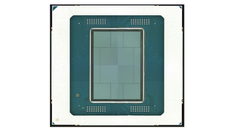
Here
is what the Monaka sample looks like:
It
is not clear exactly how Fujitsu will implement Broadcom’s 3.5D Extreme
Dimension System in Package (XDSiP) chiplet stacking – the company is saving
something to say for the launch of the Monaka chip when it comes out in 2027 –
but Bharadwaj says that Fujitsu is stacking a compute chiplet using 2 nanometer
processes atop another compute tile with 5 nanometer processes.
There
are a half dozen other companies implementing 3.5D XDSiP in their custom AI XPU
designs, says Bharadwaj. Two out of the six XPUs makers should be Amazon
Web Services with its Trainium4 due at the end of this year but probably
installing in volume in 2027 and Meta
Platforms with its MTIA 500 also due in 2027. But that is just conjecture.
“The
key thing is that customers using 3.5D XDSiP is to keep the top die in the most
advanced silicon node so that it can do the highest performance compute,” Bharadwaj
explains. “There are customers doing 3 nanometer over 3 nanometer, 2 nanometer
over 3 nanometer, and even 1.4 nanometer over 3 nanometer. That thing is kind
of evolving. The point is, putting the high performance compute at the top makes
it easier for the heat to escape, and then you put the SRAM and some low
activity compute and the interconnect at the bottom so that the heat is less
and but is still able to escape.”
Bharadwaj
says that Broadcom has been working on 3.5D XDSiP for over five years, and that
it is a different approach to the “face-to-back” 3D SoIC approach that AMD created
and developed with Taiwan Semiconductor Manufacturing Co and has used, for
instance, to stack L3 dies atop compute dies and interlink them with pins on
the chip.
Here
is what the face-to-back 3D SoIC approach looks like:
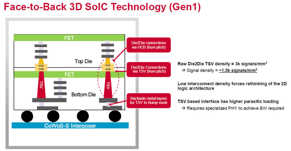
Keep
your eye on that TSV density. With face to back approaches thus far, Bharadwaj
says that you can get a signal density of maybe 1,500 signals per square
millimeter, and that means chip designers have to be mindful of the
architecture of the top and bottom chips and how they link together.
If
you go face-to-face on the chip stacking, the metal on the two dies are already
aligned, and you don’t have to do anything special in the 2D chiplet designs to
make that happen. All you need is a bonding agent to make them stay linked,
which Broadcom and TSMC have been working on together to develop 3.5D XDSiP.
Like this:
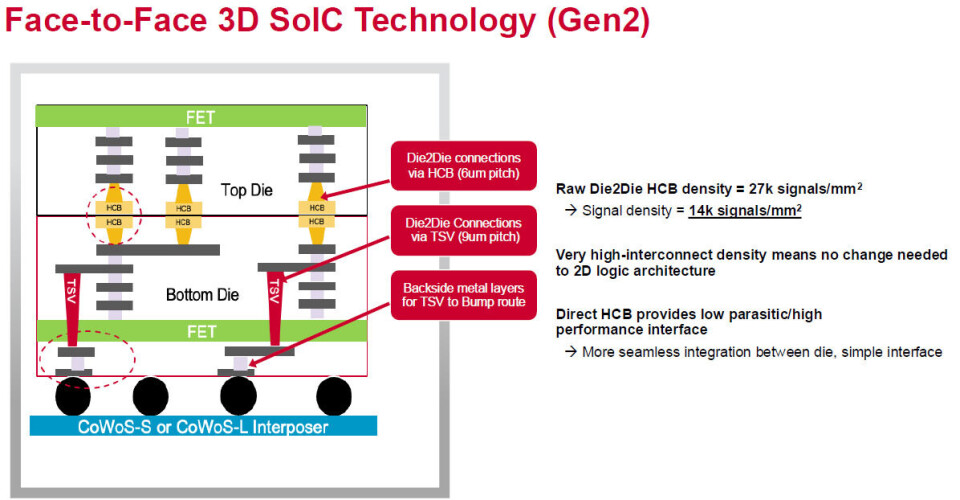
With
3.5D XDSiP, the signal density between the two chips is almost an order of
magnitude larger, with 14,000 signals per millimeter squared.
And that is why there is one CPU and six XPUs lined up
to use the technology. Fujitsu will not be the first to ship, but at least one
of the six will ship sometime in the second half of 2026 according to Broadcom.